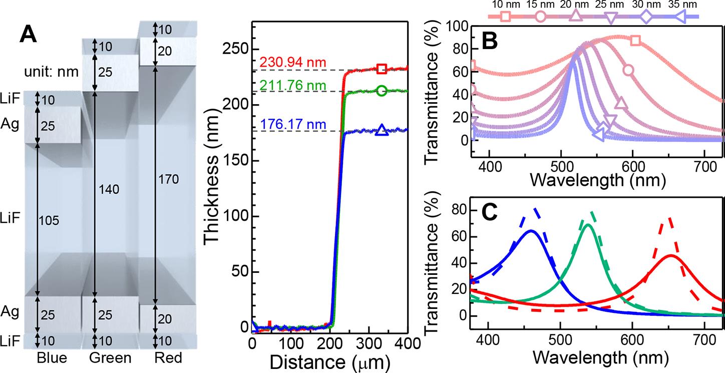
(A) Schematic illustration of etalon-electrode structures (left) and thickness profiles of the optimized R-/G-/B-selective etalonelectrodes (right), (B) simulated transmittance spectra with various Ag thicknesses, (C) transmittance spectra with respect to central optical spacer thickness (dashed line: simulated, solid line: measured). Optical spacer thickness was fixed to 140 nm in (B), and reflective electrode thicknesses were fixed to 25 nm in (C) for simulation.
A technology that has maximized space intensity by eliminating color filter from an image sensor has been developed. The National Research Foundation of Korea (Chairman Jung Hye Rho) announced that DGIST Professor Dae Sung Chung’s research team developed a color filter-free full-color image sensor using an interferometer electrode.
The image sensor used currently contains a color filter to accurately take the photo of an object. However, it has been pointed out for its shortcomings such as the declined efficiency of an electronic device, increased processing cost, and thick volume of sensor caused by the insertion of color filter.
By replacing the transparent electrode of the existing image sensor with the electrode of an interferometer structure, the research team enabled the image sensor to perform both the roles of electrode and color filter and succeeded in developing an image sensor prototype by applying this.
The research team applied the permeation of light in certain wavelength through the multiple interference in the interferometer structure. By adjusting the components and thickness of the interferometer electrode in particular, the team increased the color selectivity of Red (R) / Green (G) / Blue (B) without sacrificing electric conductivity.
The team also developed color-selective photodiodes by applying the interferometer electrode developed to a high-performance photodiode structure, which absorbs entire visible light range and produced an image sensor where these photodiodes are arranged in 10x10 pixel. The image sensor is applicable to flexible wearable devices because the thickness of its unit pixel is less than 800nm.
Professor Dae Sung Chung explained the significance of this research by stressing that “This is a technological innovation that overcame the structural limitations of existing image sensor, by achieving both color-free and thin thickness image sensor. This technology will be expanded to applications in mobile devices using not only visible rays but also near-infrared and infrared color-free image sensor.”
This research was performed with the support from the Ministry of Science and ICT as well as the Basic Research Project (mid-level research) and Core Space Technology in National Research Foundation of Korea Basic, and it was published online on ‘ACS Nano’, a world-renowned academic journal in material science, on February 1.
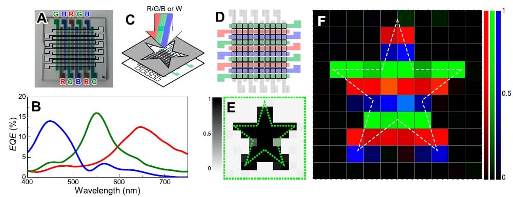
(A) Digital camera image of the fabricated 10 columns of etalon-electrodes, (B) measured EQE spectra of R-/G-/B-selective OPD pixels at −1 V, (C) a schematic illustration describing how to obtain star-shaped RGB image from R-/G-/B-selective OPD array, (D) configuration of OPD array which the R-/G-/B-pixels (black squares) were formed by sandwiching bottom R-/G-/B-selective etalonelectrodes (pastel red, green and blue) and top reflective electrode (LiF:Al, gray), (E) normalized photocurrent distribution when white light was illuminated on the OPD array through a star-shaped shadow mask, and (F) collected result of normalized photocurrent distributions when red (650 nm, 31.7 μW/cm2), green (550 nm, 29.5 μW/cm2), and blue (450 nm, 43.1 μW/cm2) lights were illuminated on the OPD array covered with a star-shaped shadow mask. In Figure 4 A,E,F, semitransparent horizontal electrode structures and green and white dotted stars were added for the reader’s convenience.