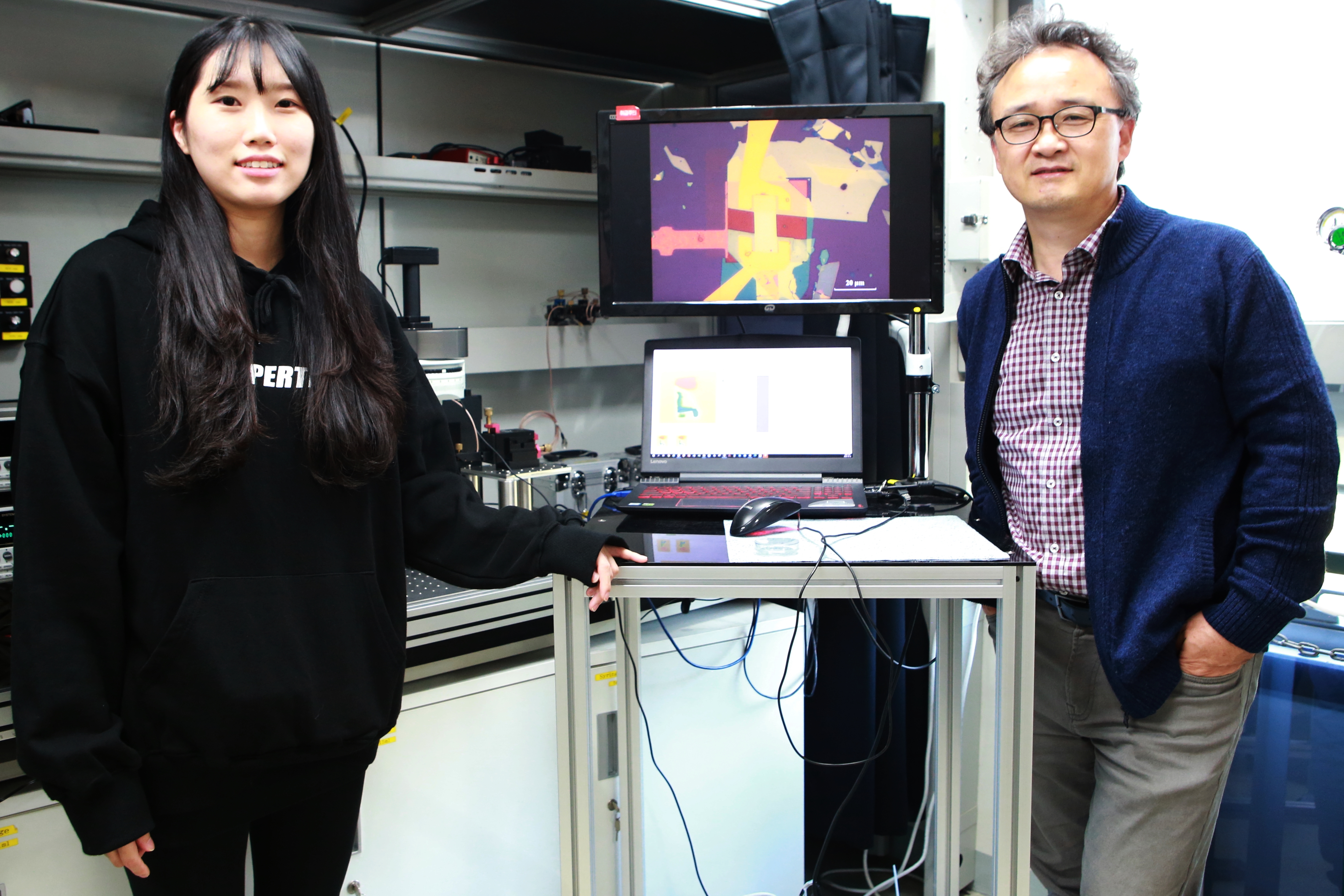
Professor Jong-Soo Lee (right) with Min-Hye Jeong (left), a student from the integrated Master & Doctorate program, next to their observation devices for the experiment
Heterojunction structures using 2D materials show immense potential in building advanced optoelectronic devices, but to use them in an optimal manner, understanding their charge properties is crucial.
Heterojunction structures composed of 2D materials are useful for designing advanced energy devices. In a new study, researchers from Daegu Gyeongbuk Institute of Science and Technology, Korea, find a way that makes it easier to build heterojunction structures. They used a technique that enabled them to dig deeper into how charge properties of the device can be regulated.
2D materials, consisting of a single layer of atoms, are revolutionizing the field of electronics and optoelectronics. They possess unique optical properties that their bulky counterparts do not, spurring the creation of powerful energy devices (for example, optic fibers or solar cells). Interestingly, different 2D materials can be stacked together in a “heterojunction” structure, to generate light-induced electric current (or “photocurrent”). To do this in an optimal manner, it is important to find the right “balance” of the charged particles (called “electrons” and “holes”) and the energy produced by them.
While chemically treating the surface of the materials (“chemical doping”) can help to some extent, this technique is not very efficient in 2D materials. Another solution is to control the charge properties by tuning the voltage in a precise manner, a technique called “electrostatic doping.” This technique, however, needs to be explored further.
A team of researchers from Daegu Gyeongbuk Institute of Science and Technology, Korea, led by Professor Jong-Soo Lee, set out to do this, in a studypublished in Advanced Science. For this, they built a multifunctional device, called a “phototransistor,” composed of 2D heterojunctions. The main strategy in their design was the selective application of electrostatic doping to a specific layer.
Prof Lee further explains the design of their model, “We fabricated a multifunctional 2D heterojunction phototransistor with a lateral p-WSe2/n-WS2/n-MoS2 structure to identify how photocurrents and noise were created in heterojunctions. By controlling the electrostatic conditions in one of the layers (n-WS2), we were able to control the charge that was carried to the other two layers.”
The fact that the researchers could control the charge balance enabled them to observe the origin of the photocurrent as well as of the unwanted “noise” current, using a photocurrent mapping system. They could also study the charges in relation to the conditions that they set. But the most interesting part was that when the concentration of charge was optimal, the heterojunction structure showed faster and higher photoresponsivity as well as higher photodetectivity!
These findings shed light on the importance of charge balance in heterojunctions, potentially paving the way for advanced optoelectronic devices. Prof Lee concludes, “Our study reveals that even if the charge densities of the active materials of the layered structures are not perfectly matched, it is still possible to create an optoelectronic device having excellent characteristics by tuning the charge balance through the gate voltage.”
Reference
|
Authors: |
Hyun-Soo Ra,1 Min-Hye Jeong,1 Taegeun Yoon,2,3 Seungsoo Kim,2 Young Jae Song,2,3 and Jong-Soo Lee1 |
|
Title of original paper: |
Probing the Importance of Charge Balance and Noise Current in WSe2/WS2/MoS2 van der Waals Heterojunction Phototransistors by Selective Electrostatic Doping |
|
Journal: |
Advanced Science |
|
DOI: |
10.1002/advs.202001475 |
|
Affiliations: |
1 Department of Energy Science and Engineering Daegu Gyeongbuk Institute of Science and Technology (DGIST), Republic of Korea 2Department of Nano Engineering Sungkyunkwan University (SKKU), Korea 3SKKU Advanced Institute of Nano Technology (SAINT), Sungkyunkwan University (SKKU), Korea
|
*Corresponding author’s email: [email protected]
About Daegu Gyeongbuk Institute of Science and Technology (DGIST)
Daegu Gyeongbuk Institute of Science and Technology (DGIST) is a well-known and respected research institute located in Daegu, Republic of Korea. Established in 2004 by the Korean Government, the main aim of DGIST is to promote national science and technology, as well as to boost the local economy.
With a vision of “Changing the world through convergence", DGIST has undertaken a wide range of research in various fields of science and technology. DGIST has embraced a multidisciplinary approach to research and undertaken intensive studies in some of today's most vital fields. DGIST also has state-of-the-art-infrastructure to enable cutting-edge research in materials science, robotics, cognitive sciences, and communication engineering.