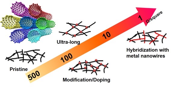
Figure Progress of pristine carbon nanotubes towards carbon nanotube based transparent conductive films. Copyright 2016 Ying Zhou and Reiko Azumi
Scientists are developing flexible, stretchable and wearable optoelectronic devices, such as body sensors that could provide continuous monitoring of a person’s blood pressure. However, the jury is still out on the best materials to use for manufacturing these devices. Carbon nanotubes (CNTs) show promise and some challenges.
Ying Zhou and Reiko Azumi from Japan’s National Institute of Advanced Industrial Science and Technology reviewed the latest research on the use of carbon nanotubes in manufacturing an important component of optoelectronic devices called transparent conductive films (TCFs). These are thin films of a material that is optically transparent and electrically conductive. The market for TCFs is expected to reach 1.2 billion dollars by 2025. Currently, they are manufactured using indium tin oxide (ITO), which has the advantage of excellent electrical conductive properties but the disadvantage of poor flexibility, making it unsuitable for wearable devices.
Researchers are investigating several ITO alternatives for manufacturing TCFs. Carbon nanotube-based devices are among those showing promise. CNTs are nanosized cylindrical tubes with high theoretical electrical conductivity. CNTs have dropped in price due to their commercialization for applications such as water filtration systems, sports equipment, and batteries and conductors, for example, and prices could be further reduced by improving manufacturing processes.
Sensing devices, such as wearable touch panels, are the most promising application for CNT-based transparent conductive films. Two companies in Japan are already using CNTs to manufacture touch panels for mobile electronics. Organic LEDs (OLEDs), which are already used to manufacture thinner, lighter and more efficient TV screens, are another promising application for CNT-based TCFs. But other materials used in their manufacture, such as metal nanowires, have higher conductivity and transparency and thus result in a better performance.
“Based on the overview of the fabrication, properties and possible applications of CNT-based TCFs, it can be concluded that current CNT-based TCFs still do not meet the demands of performance/cost for industrial use,” write the researchers in their review published in the journal Science and Technology of Advanced Materials. Manufacturing costs need to be reduced while their conductivity and transparency need to be improved, they say.
The researchers recommend future investigations build on the flexibility and stretchability of CNT-based TCFs by improving their manufacturing and conductivity to make them worthy contenders for wearable optoelectronics.
For further information please contact:
Dr. Ying Zhou
Photonics and Electronics Research Institute,
National Institute of Advanced Industrial Science and Technology
Tsukuba, Ibaraki 305-8565, Japan
E-mail: [email protected]
Prof. Reiko Azumi
Photonics and Electronics Research Institute
National Institute of Advanced Industrial Science and Technology
Tsukuba, Ibaraki 305-8565, Japan
E-mail: [email protected]
Article information
Ying Zhou and Reiko Azumi: “Carbon nanotube based transparent conductive films: progress, challenges, and perspectives”, Science and Technology of Advanced Materials Vol. 17 (2016) p. 1214526.
http://dx.doi.org/10.1080/14686996.2016.1214526
Journal information
Science and Technology of Advanced Materials (STAM) is an international open access journal in materials science. The journal covers a broad spectrum of topics, including synthesis, processing, theoretical analysis and experimental characterization of materials. Emphasis is placed on the interdisciplinary nature of materials science and on issues at the forefront of the field, such as energy and environmental issues, as well as medical and bioengineering applications
For more information about STAM contact:
Mikiko Tanifuji
Publishing Director
Science and Technology of Advanced Materials
E-mail: [email protected]